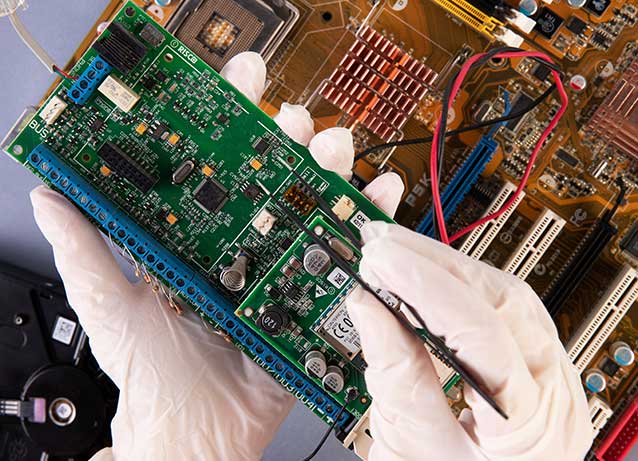
This section should capture the department’s capability to electrically, thermally, and functionally characterize semiconductor devices, nanoelectronic structures, and related materials / stacks. These labs are especially important for faculty working on GaN, advanced Si, 2D materials, memory devices, sensors, and reliability.
The page may be structured around functional classes such as probe-station-based measurements, low-noise characterization, pulsed and transient measurements, temperature-dependent measurements, nanoscale imaging / inspection links, and device reliability / performance evaluation. Where multiple faculty groups have related characterization capability, the page should present this as a department-wide asset rather than fragmented islands.